FPGA Mezzanine Card DSP Module
We would like to present an outline of our project which is ”FPGA Mezzanine Card DSP Module”.
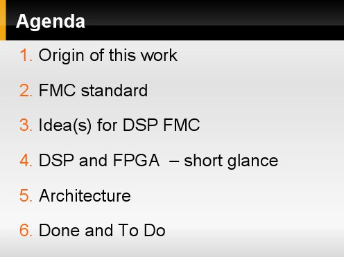
Plan of our presentation consists of:
- Short introduction to what this card is being made for,
- A glance into the FMC standard,
- Sterssing out main assumptions and general solution scheme,
- Short characteristic of chosen DSP and FPGA,
- Presenting the architecture we came up with,
- And finnaly pointing out ”Done and To Do list”.
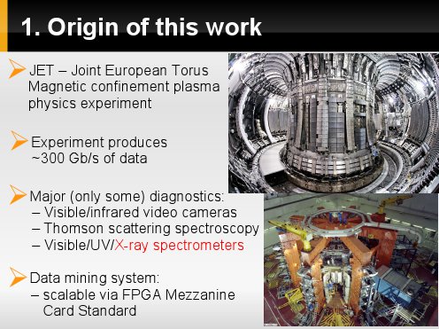
Origin of our project comes from the JET experiment, which is a plasma physics experiment, that from our point of view, produces huge ammount of data to be processed.
JET is equipped with many diagnostics systems some of which are pointed out here.
Data mining system has been proposed that is scalable using FPGA Mezzanine Card Standard.
Our project is to be used as a part of this data mining system. Namely to boost up the X-ray spectrometer calculations by using the DSP FMC accelerator module.

A quick overview of the FMC standard
This standard defines two shapes of FMC plugin module, single width, and double width. We focus on single width module. An example is shown on the picture here. The idea is very simple like in other Mezzanine cards -- to add functionality to the carrier cards by pluging in the FMC module.
For the plug-in purposes, FMC standard specifies Samtec’s SEARAY™ connector set.
Standard also defines two pinout versions for this connector
Low–Pin count and High–Pin count.
Low-pin count comes with 160 pins. High-pin count comes with 400 pins.
The main differences are pointed out here on the page
Low–Pin count is a subset of high–pin count
and is mechanically compatible with High–Pin connector.
The pinout consist mainly of dedicated:
- clock pins,
- JTAG pins,
- I2C pins,
- power pins,
- transciever pins,
- and user defined signal pairs.
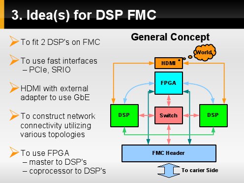
To fulfill the aim of the project we came up with some basic assumptions:
- first, to fit 2 DSP's on our module, it's not many but still they make a cluster,
- second, to use fast and digital only interfaces,
- third, to construct different types of connectivity, allowing to chose one that suits a particular algorithn the best,
- and the last one, to use FPGA which could be working as: a master to DSP's or as coprocessor to DSP's.
General solution scheme is shown here on a picture. We can see two processors – connected via point to point link, by a switch, by FPGA and possibly by ethernet.
FPGA and the switch in the end, are connected to the FMC header for exchanging data with the carier board.
To realize our basic solution scheme many different DSP's and FPGA's can be used.
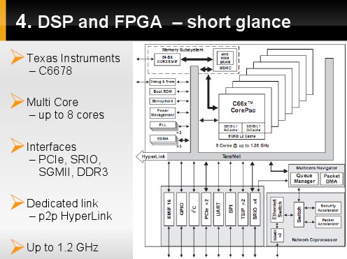
In place of DSP we had chosen, possibly today's fastest, TMS C66 78 from Texas Instruments.
DSP's insides are shown on the picture here.
This DSP has fast interfaces like:
- PCI expess,
- SGM double I allowing for gigabit ehternet,
- Serial Rapid-IO,
- dedicated point-to-point link,
Computing power of all 8-cores is calculated to be 160 GFLOPs
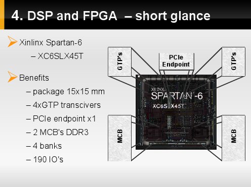
In place of FPGA we had chosen Spartan-6 from Xilinx.
FPGA was chosen to be possibly the smallest and yet having possiblity to connect it to fast interfaces like PCI express, Serial RApid-IO and DDR 3 interface.
Above to that, FPGA comes handy to utlize free IOs as FMC's user-defined singals – that is where 190 IO's are useful
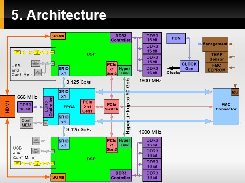
Architecture we came up with is shown on the picture, additionally possible transfer speeds are also shown.
In few words:
- the managment block controls and suprevises power network and clock distribution,
- when FPGA is powered up and programmed using FLASH or JTAG -- it configures DSPs for bootloading via for instance FLASH , ethernet or PCI express,
- additonally to all the fast interfaces, there is also UARTs translated to USB for debugging purposes,
- the central point of this board is the PCI express switch that uses packet header information for how and where to pass the data -- it is called a non-blocking switch,
- every unit capable of processing is equipped with RAM memories allowing for wider spectrum of algorithms to be implemented,
- in the the end, we can see a mesh network-like connectivity.
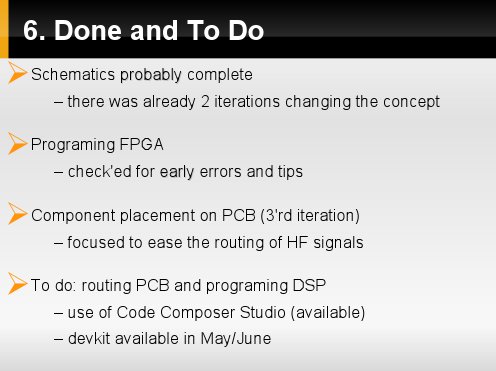
This is the first semester of this project and schematics are almost complete. We aim to design schematics before the end of February.
This might need some redesigning in the future however, becuse chosen DSP still has an experimental staus
3 last steps lies ahead of us:
- programing FPGA, which might catch critical errors, so that we could redisgn the schemtacis before completing PCB layout,
- offcourse to do PCB layout, which might be hard due to fast interfaces and lack of producent provided FPGA and DSP PCB libraries,
- and final step to program and test the borad.
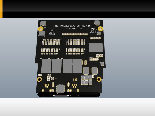
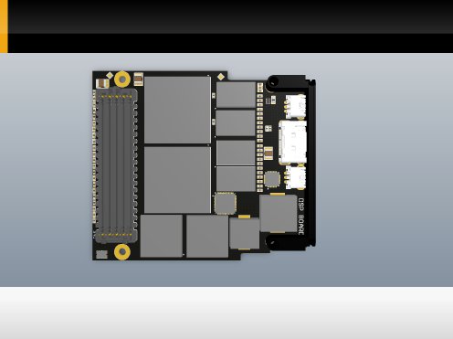
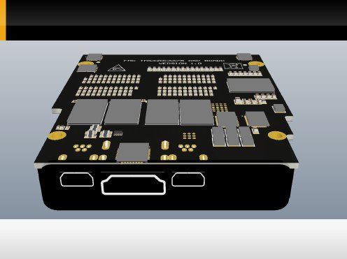
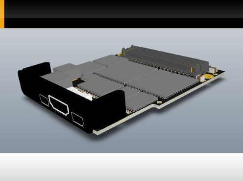
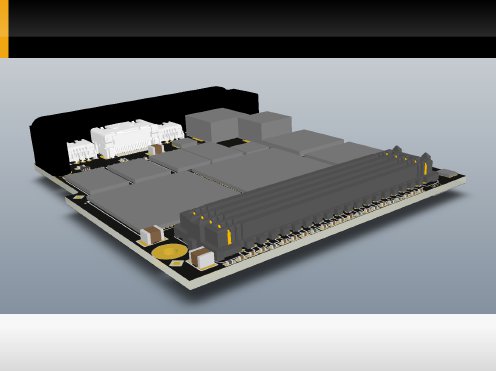
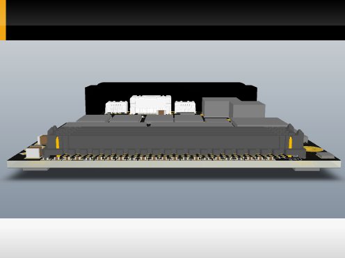
This is a 3D model of the propsoed PCB from diffretent POVs.
| Attachment | Wielkość |
|---|---|
| FPGA Mezzanine Card DSP Module [2011].pdf | 4.17 MB |